


Hotline
+86 13310681862
Description:
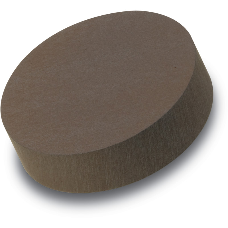
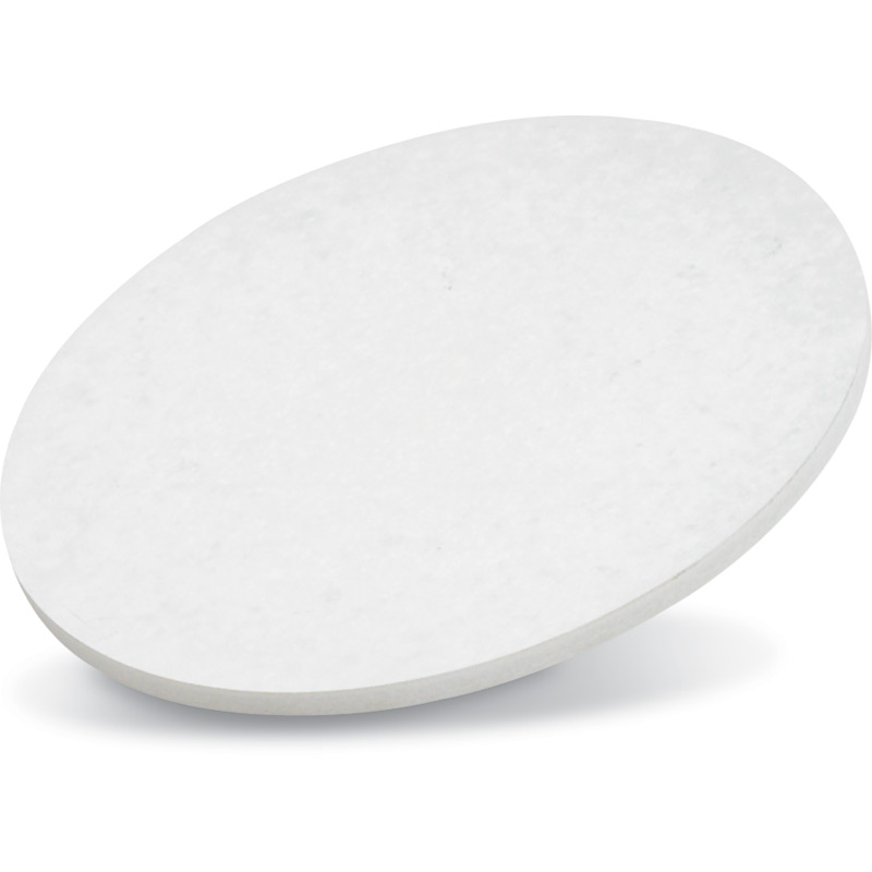
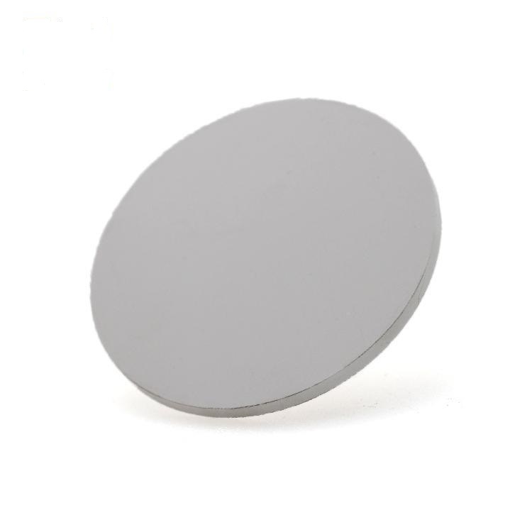
Boron Doped Aluminum Nitride (Al0.93B0.07N) Sputtering TargetAluminum Boron Nitride (Al₀.₉₃B₀.₀₇N) Sputtering Targets: Enabling Next-Generation Functional Thin Films for Advanced ResearchAluminum Boron Nitride (Al₀.₉₃B₀.₀₇N) sputtering targets represent a cutting-edge class of ceramic ma...
Aluminum Boron Nitride (Al₀.₉₃B₀.₀₇N) sputtering targets represent a cutting-edge class of ceramic materials engineered to
deposit high-performance nitride thin films. By incorporating boron into the aluminum nitride lattice,
these targets yield films with enhanced piezoelectric response, thermal stability, and wide-bandgap semiconductor properties.
This makes AlBN an ideal material platform for pioneering research in microelectronics, photonics, energy harvesting,
and extreme-environment applications. Below, we outline key domains where AlBN thin films demonstrate significant scientific
and technological promise.
◼️ 1. High-Frequency Acoustic Wave Devices
AlBN films excel as piezoelectric layers for high-frequency surface acoustic wave (SAW) and bulk acoustic wave (BAW) resonators.
Their high acoustic velocity and electromechanical coupling coefficient enable:
5G/6G RF Filters: Supporting ultra-wideband frequencies with reduced signal loss and improved power handling for next-generation communication systems.
Microacoustic Sensors: Facilitating high-sensitivity gas, pressure, or biosensors due to enhanced piezoelectric response and
thermal stability compared to conventional AlN films.
◼️ 2. Piezoelectric MEMS and Energy Harvesting
The superior piezoelectric coefficient and thermal resilience of AlBN films advance microelectromechanical systems (MEMS) research:
Energy Harvesters: Enabling efficient vibration-to-electricity conversion in high-temperature environments
(e.g., industrial or aerospace settings).
Precision Actuators: Supporting low-drive-voltage MEMS mirrors, switches, and nanopositioners for photonics and
nanomanipulation applications.
◼️ 3. Ultraviolet (UV) Photonics and Optoelectronics
AlBN’s tunable wide-bandgap properties (up to ~6.2 eV) position it as a candidate for UV-centric devices:
Solar-Blind UV Detectors: Serving as active layers for deep-UV sensing free from visible-light interference.
UV-Transparent Electrodes: Enabling conductive yet optically transparent components for UV-LEDs and laser diodes.
◼️ 4. Protective and Tribological Coatings
AlBN films exhibit exceptional hardness and oxidation resistance, driving research in:
Hard Coatings for Cutting Tools: Extending service life of high-speed machining tools under thermal/mechanical stress.
Corrosion-Resistant Barriers: Protecting sensitive components in aggressive chemical or high-humidity environments.
◼️ 5. High-Temperature and Harsh-Environment Electronics
The stability of AlBN films at elevated temperatures supports innovations in:
Wide-Bandgap Power Devices: Serving as insulating or passivation layers for GaN- or SiC-based electronics.
Embedded Sensors: Enabling strain or temperature monitoring in jet engines, nuclear systems, and energy reactors.

Warmly welcome new and regular customers' inquiry!
Contact Us
ICP:鲁ICP备18046268号-1 鲁公网安备37048102006786号 XMLMap
Address:New Business Building, Tengzhou City, China
