


Hotline
+86 13310681862
Description:
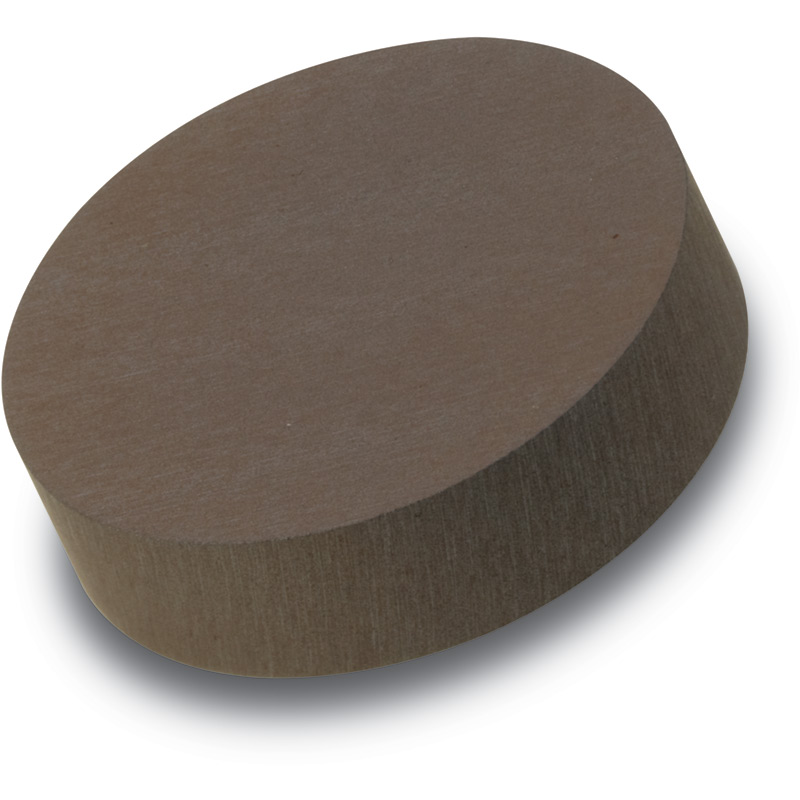
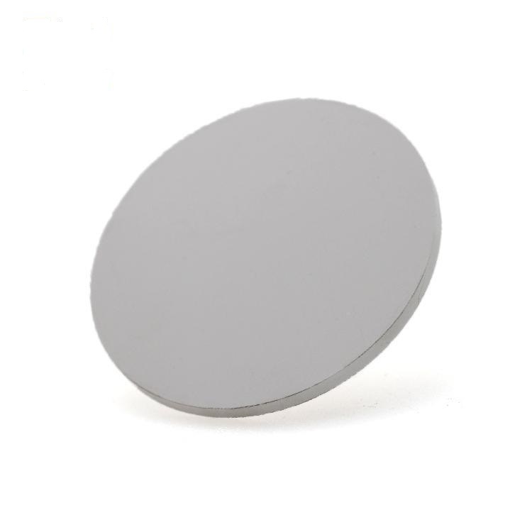
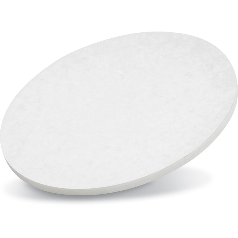
Silicon Nitride (Si3N4) Sputtering TargetApplications of Si3N4 sputter target:1. Semiconductor & MicroelectronicsHigh-k Dielectric Layers: Si₃N₄ films act as insulating barriers in transistors and memory devices, enhancing capacitance while minimizing leakage currents due to their high dielect...
1. Semiconductor & Microelectronics
High-k Dielectric Layers: Si₃N₄ films act as insulating barriers in transistors and memory devices, enhancing capacitance while minimizing leakage
currents due to their high dielectric strength.
Anti-Reflective Coatings (ARC): Critical for photolithography, Si₃N₄ layers suppress reflection at 193–365 nm wavelengths, improving pattern
resolution in EUV and deep-UV lithography.
Passivation Layers: Protect silicon wafers from ionic contamination and moisture, significantly extending device reliability.
2. Optics & Photonics
Low-Loss Waveguides: With near-zero optical absorption from UV to IR, Si₃N₄ films enable high-density photonic integrated circuits (PICs),
outperforming SOI waveguides by 3–4 orders of magnitude in loss reduction.
Anti-Reflective & UV-Blocking Coatings: Optimize transmission for lenses, solar cells, and displays while providing durable surface protection.
3. Renewable Energy
Solar Cell Passivation: Si₃N₄ coatings on photovoltaic panels reduce reflection losses and serve as moisture/chemical barriers, boosting efficiency and lifespan.
Fuel Cell Components: Thin films enhance corrosion resistance in bipolar plates and membrane electrodes, particularly in alkaline environments68.
4. Advanced Functional Coatings
Wear-Resistant Layers: For cutting tools, bearings, and aerospace components, leveraging hardness (>1,500 HV) and low friction coefficients.
Biocompatible Interfaces: Used in medical implants and surgical tools due to bio-inertness and antibacterial properties.
5. Emerging Research Domains
Power Electronics: Enables direct bonding of Cu-Si₃N₄ substrates for high-temperature, void-free insulated circuit boards, replacing traditional AMB techniques.
Quantum Sensors: Low-stress Si₃N₄ membranes serve as interferometer components in gravity-wave detectors.
For questions about target material or anything we can hlep, please click here.
| Specifications | |||
| Material Type | Silicon Nitride | ||
| Symbol | Si3N4 | ||
| Purity | 99.9% | ||
| Size | 1.00" Dia. x 0.125" Thick ~8.00" Dia x 0.250" Thick / Custom | ||
| Package Unit | 1pc | ||
| Theoretical Density (g/cc) | 3.44 | ||
| Melting Point (°C) | 1,900 | Sputter | RF, RF-R |
| Type of Bond | Indium, Elastomer | Max Power Density (Watts/Square Inch) | 20* |
Warmly welcome new and regular customers' inquiry!
Contact Us
ICP:鲁ICP备18046268号-1 鲁公网安备37048102006786号 XMLMap
Address:New Business Building, Tengzhou City, China
