


Hotline
+86 13310681862

Description:
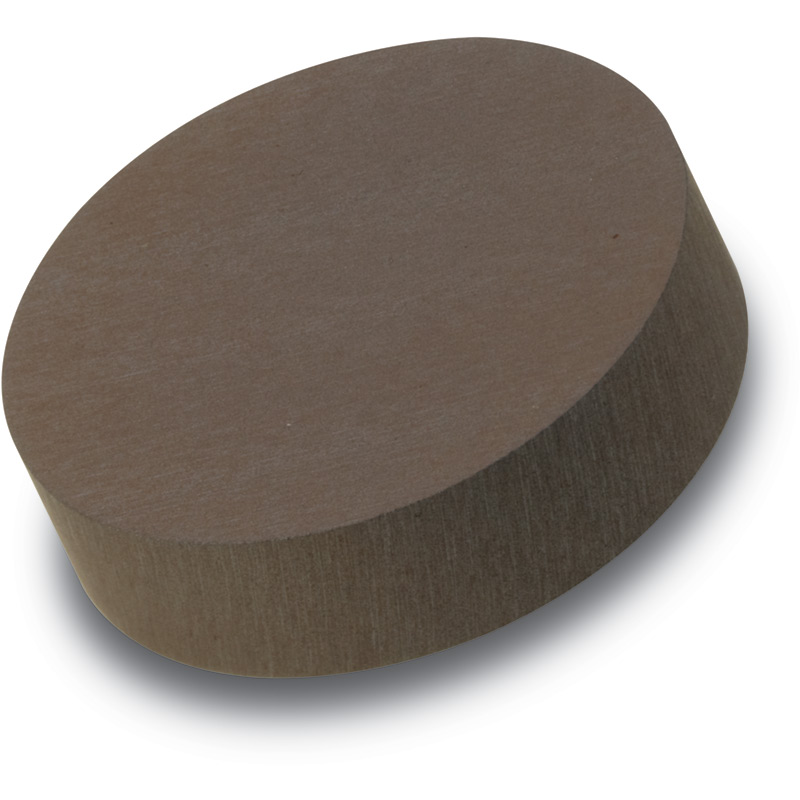
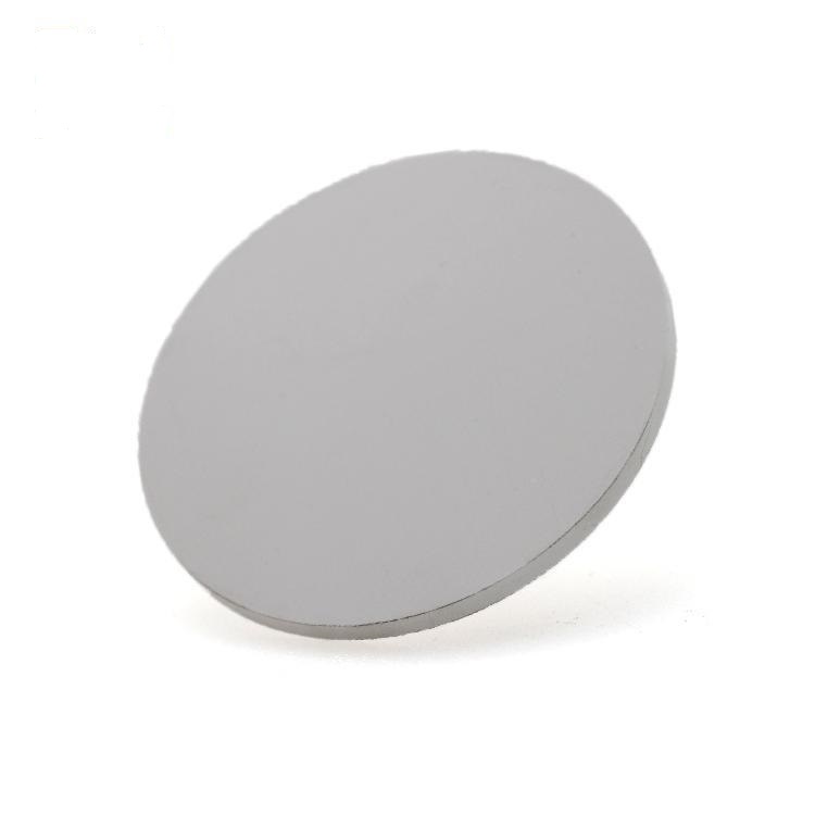
Indium Oxide (In2O3) Sputtering TargetIndium oxide (In₂O₃) sputtering targets are indispensable in thin-film technology for synthesizing high-performance functional layers. Below is a detailed overview of their key applications, supported by cutting-edge studies from international academic journal...
Indium oxide (In₂O₃) sputtering targets are indispensable in thin-film technology for synthesizing high-performance functional layers.
Below is a detailed overview of their key applications, supported by cutting-edge studies from international academic journals:
1. Thin-Film Transistors (TFTs) and Display Technology
High-Mobility TFTs: In₂O₃ films deposited via sputtering enable polycrystalline transistors with field-effect mobility exceeding 139 cm²·V⁻¹·s⁻¹
after hydrogenation and low-temperature solid-phase crystallization (SPC). This outperforms amorphous silicon and competes with low-temperature polysilicon (LTPS),
making them ideal for next-generation displays and flexible electronics.
Ultra-Thin Channel Layers: Atomic-layer-deposited (ALD) amorphous In₂O₃ films (0.7–1.5 nm thick) exhibit tunable threshold voltages and high on/off ratios (>10⁷).
This scalability addresses back-end-of-line (BEOL) compatibility for monolithic 3D integration in advanced microelectronics.
2. Transparent Conductive Electrodes and Optoelectronics
Doped In₂O₃ Systems: Co-sputtering with dopants (e.g., Mg, Sn, Zn) optimizes electrical and optical properties. For instance:
Mg-doped In₂O₃ (In₂O₃:Mg) enhances UV photodetection, achieving a responsivity of 2.6 A/W and UV-visible rejection ratios up to 4.8×10⁵.
Sn-doped In₂O₃ (ITO) and In₂O₃–SnO₂–ZnO ternary targets produce low-resistivity films for solar cells and touch panels
3. Gas Sensors
Heterostructured Nanosensors: Electrospun In₂O₃/α-Fe₂O₃ nanotubes exhibit high ethanol sensitivity (ppm-level detection) and fast response/recovery
at low operating temperatures. The cubic In₂O₃ nanocrystals enhance surface reactivity, enabling ultrasensitive chemiresistive sensors.
4. Photocatalysis and Energy Applications
S-Scheme Heterojunctions: MOF-derived CuO@In₂O₃ core-shell structures facilitate efficient CO₂-to-fuel conversion. The In₂O₃ shell promotes charge separation,
achieving 3× higher activity than pristine oxides.
Bandgap Engineering: Co-doping In₂O₃ with transition metals (e.g., Co) tailors electronic structures without altering bandgaps significantly, benefiting photoelectrochemical devices.
| Specifications | |||
| Material Type | Indium Oxide | ||
| Symbol | In2O3 | ||
| Purity | 99.99% | ||
| Size | 1.00" Dia. x 0.125" Thick ~8.00" Dia x 0.250" Thick / Custom | ||
| Package Unit | 1pc | ||
| Theoretical Density (g/cc) | 7.18 | ||
| Melting Point (°C) | 2000ºC | Sputter | RF, DC |
| Type of Bond | Indium, Elastomer | Max Power Density (Watts/Square Inch) | -- |
Warmly welcome new and regular customers' inquiry!
Contact Us
ICP:鲁ICP备18046268号-1 鲁公网安备37048102006786号 XMLMap
Address:New Business Building, Tengzhou City, China
