


Hotline
+86 13310681862

Description:
Indium Gallium Zinc Oxide IGZO Sputter TargetsIGZO (Indium Gallium Zinc Oxide) sputtering targets represent a class of high-performance oxide semiconductor materials essential for depositing functional thin films. These targets enable precise fabrication of IGZO films with exceptional electronic and...
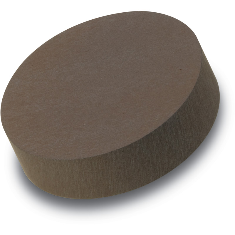
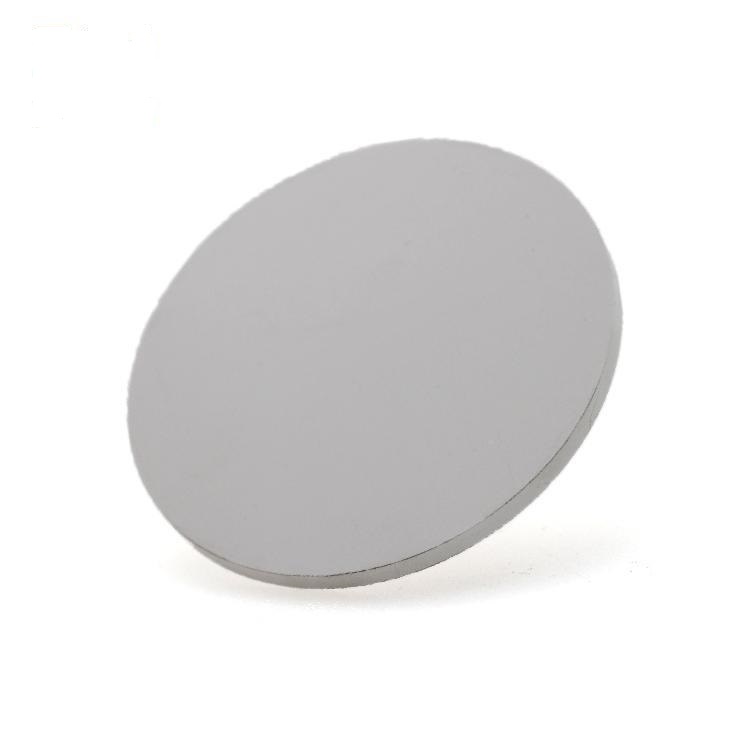
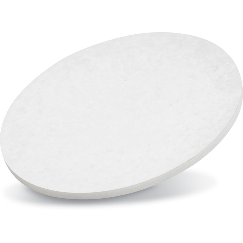
Indium Gallium Zinc Oxide IGZO Sputter Targets
IGZO (Indium Gallium Zinc Oxide) sputtering targets represent a class of high-performance oxide semiconductor materials
essential for depositing functional thin films. These targets enable precise fabrication of IGZO films with exceptional electronic
and optical properties, making them indispensable for next-generation devices in multidisciplinary research. Below we outline
their key application domains relevant to academic and industrial R&D laboratories.
1. Thin-Film Transistors (TFTs) for Advanced Displays
IGZO films deposited via magnetron sputtering are widely adopted as channel layers in TFTs due to their high carrier mobility,
low off-state current, and superior uniformity over large areas. These properties drive research in:
High-Resolution Displays: Enabling ultra-HD micro-OLEDs and LCDs with enhanced pixel response speeds and reduced power
consumption.
Flexible Electronics: Facilitating low-temperature processing compatible with heat-sensitive polymer substrates for
bendable/foldable displays.
Stability Engineering: Investigating passivation layers (e.g., AlOₓ) and annealing processes to improve TFT stability
against electrical/optical stress.
2. Transparent Electrodes & Optoelectronic Devices
The tunable optoelectronic properties of IGZO films support applications demanding balanced conductivity
and transparency:
Infrared (IR) Optoelectronics: Serving as transparent electrodes in SWIR (short-wave infrared) sensors due
to broadband transparency from visible to IR regions.
Multi-Layer Stacks: Enabling low-stress, amorphous films with smooth surfaces for complex optical coatings
in photodetectors and imaging systems.
3. Photovoltaic & Energy Devices
IGZO’s bandgap engineering and defect tolerance make it attractive for energy conversion/storage research:
Solar Cell Electrodes: Functioning as transparent conductive layers in CIGS and perovskite solar cells.
Thin-Film Battery Components: Depositing interfacial layers to enhance charge transport in solid-state lithium batteries.
4. Emerging & Flexible Electronics
The compatibility of IGZO with non-conventional substrates unlocks novel device architectures:
Wearable Sensors: Enabling transparent, flexible circuits for biosensing and health monitoring.
Printed Electronics: Serving as a benchmark material for hybrid printed-sputtered TFT development
| Specifications | |||
| Material Type | Indium Gallium Zinc Oxide | ||
| Symbol | In2O3:Ga2O3:ZnO=1:1:1 at% | ||
| Purity | 99.99% | ||
| Size | 1.00" Dia. x 0.125" Thick ~8.00" Dia x 0.250" Thick / Custom | ||
| Package Unit | 1pc | ||
| Theoretical Density (g/cc) | 6.5 | ||
| Melting Point (°C) | 850 °C | Sputter | RF, DC |
| Type of Bond | Indium, Elastomer | Max Power Density (Watts/Square Inch) | -- |
Warmly welcome new and regular customers' inquiry!
Contact Us
ICP:鲁ICP备18046268号-1 鲁公网安备37048102006786号 XMLMap
Address:New Business Building, Tengzhou City, China
