


Hotline
+86 13310681862

Description:
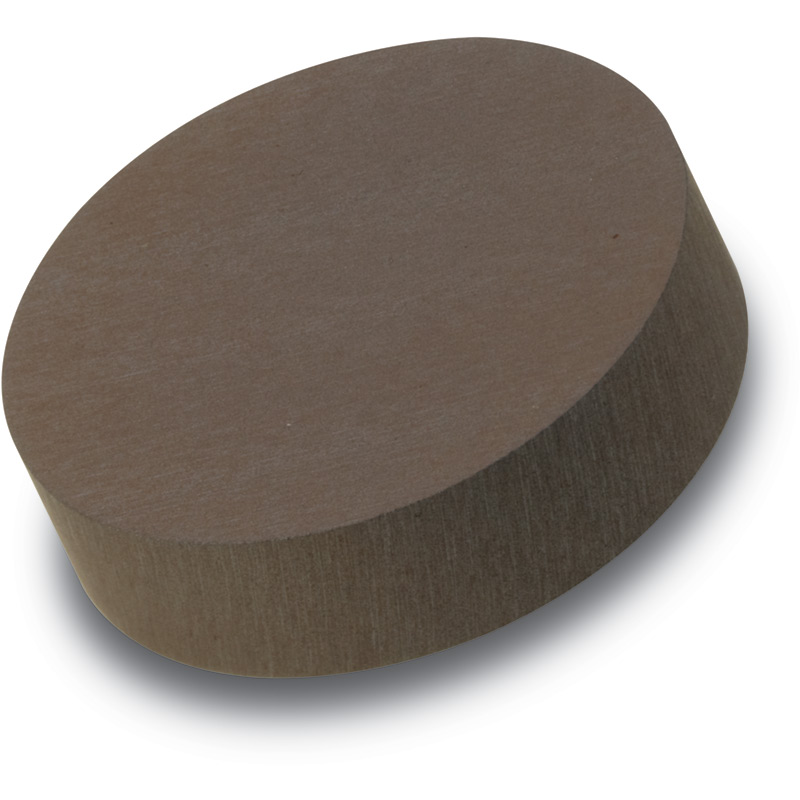
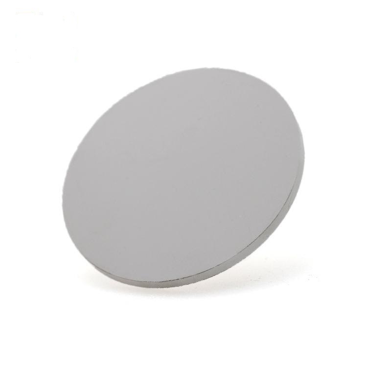
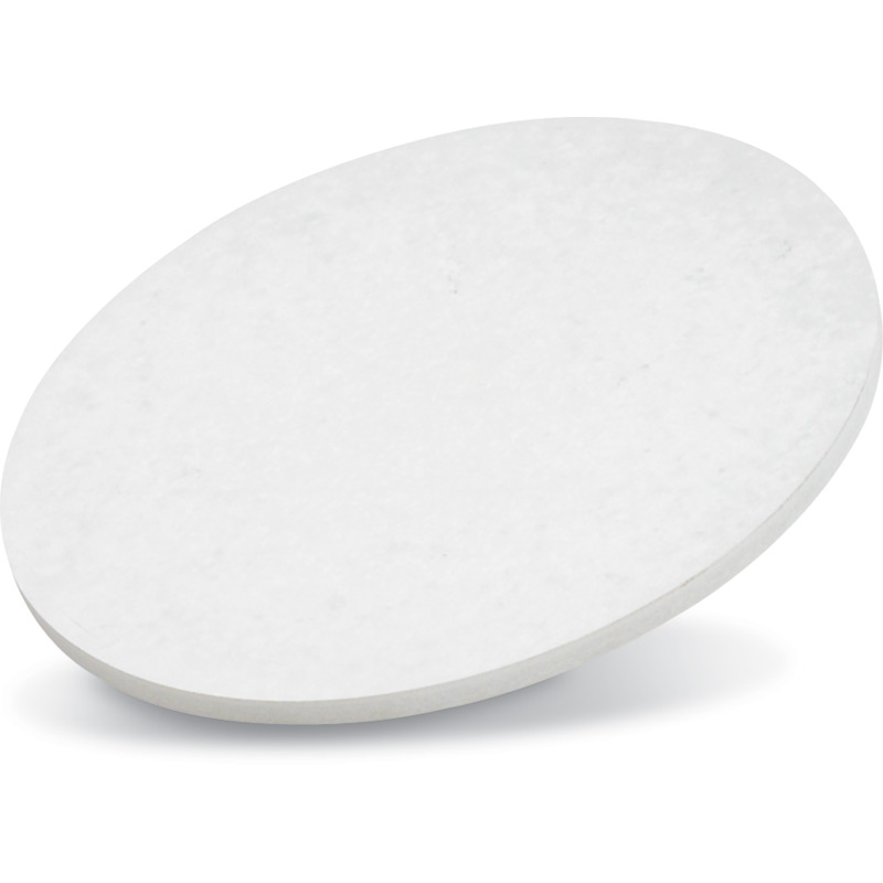
Bismuth Selenide (Bi₂Se₃) Sputtering TargetBi₂Se₃ Targets for Advanced Thin Film ApplicationsBi₂Se₃ (Bismuth Selenide) is a significant topological insulator (TI) and functional material characterized by an insulating bulk and highly conductive, spin-polarized surface states. Its unique electr...
Bi₂Se₃ Targets for Advanced Thin Film Applications
Bi₂Se₃ (Bismuth Selenide) is a significant topological insulator (TI) and functional material characterized by an insulating bulk and highly conductive,
spin-polarized surface states. Its unique electronic and optical properties make it a compelling choice for both fundamental research and
next-generation technologies. When utilized as a sputtering or evaporation target, Bi₂Se₃ enables the precise deposition of high-quality thin films
essential for exploring novel quantum phenomena and developing advanced devices.
The subsequent sections detail the primary research applications of thin films fabricated from Bi₂Se₃ targets.
🔬 1. Topological Insulator and Spintronics Research
As a prototypical 3D topological insulator, Bi₂Se₃ thin films exhibit robust, spin-momentum-locked surface states, which are protected against
back-scattering by time-reversal symmetry. These properties are critical for spintronic applications, where the goal is to manipulate electron spin
rather than charge for more efficient computing.
Key Properties: Strong spin-orbit coupling, non-trivial topological surface states, and high charge carrier mobility.
Research Applications:
Investigation of the Quantum Spin Hall Effect and other topological phenomena.
Generation and detection of spin-polarized currents for low-power spin filters and spin-transfer torque devices.
A 2023 study on MBE-grown Bi₂Se₃ films demonstrated the generation of a measurable spin photocurrent at room temperature via the Circular
Photogalvanic Effect (CPGE), highlighting its potential for room-temperature spintronic operations .
Sputtered Bi₂Se₃ films with nanoscale features have shown an 18-fold increase in computing and memory efficiency compared to conventional
materials, indicating promise for magnetic random-access memory (MRAM) .
💡 2. Advanced Photonics and Optoelectronics
Bi₂Se₃'s narrow bandgap (~0.3 eV) and high charge carrier mobility make it highly responsive to a broad spectrum of light, from visible to infrared.
This allows for the development of high-performance photodetectors and other optoelectronic components.
Key Properties: Ultra-fast charge transport, strong infrared light absorption, and excellent photoresponse .
Research Applications:
High-Speed Photodetectors: Fabrication of photodetectors on flexible substrates and silicon for visible and near-infrared (NIR) sensing.
Controlled Nanostructures: Chemical Vapor Deposition (CVD) can produce thin films with vertically aligned Bi₂Se₃ nanosheets.
This specific structure creates a large surface-to-volume ratio, enhancing light-matter interaction and yielding a strong photoresponse,
ideal for NIR photodetection .
Photoelectronic Devices: Exploration of novel device architectures that leverage the coupling between light and Bi₂Se₃'s topological surface states.
☀️ 3. Energy Solutions: Solar Cells and Thermoelectrics
Beyond its quantum properties, Bi₂Se₃ is a compelling material for energy applications, particularly as a cost-effective catalyst in solar cells
and for its intrinsic thermoelectric capabilities.
Key Properties: High electrocatalytic activity, good electrical conductivity, and a high Seebeck coefficient.
Research Applications:
Counter Electrodes in Dye-Sensitized Solar Cells (DSSCs): Bi₂Se₃ thin films, deposited via methods like MBE, can serve as highly efficient
alternatives to expensive platinum counter electrodes. Research has demonstrated DSSCs with a photoconversion efficiency of 4.35%,
competitive with traditional platinum-based cells .
Thermoelectric Devices: Research focuses on optimizing the thermoelectric figure of merit (zT) in Bi₂Se₃ films for solid-state waste
heat recovery and localized cooling in microelectronics.
🧬 4. Biomedical Nanotechnology
The biocompatibility and unique physicochemical properties of Bi₂Se₃ have opened new avenues in nanomedicine, particularly in cancer
theranostics (therapy and diagnostics).
Key Properties: High atomic number (Z) of Bismuth for strong X-ray attenuation, biocompatibility, degradability, and high photothermal
conversion efficiency .
Research Applications:
Radiosensitizers for Cancer Therapy: Two-dimensional Bi₂Se₃ nanosheets functionalized with tumor-targeting ligands (e.g., RGD peptides)
can accumulate in tumor tissue. Upon exposure to X-rays, they significantly enhance radiation dose delivery, induce cancer cell apoptosis,
and suppress tumor growth while minimizing damage to healthy tissues .
Photoacoustic Imaging (PAI): The strong NIR absorption and photothermal conversion efficiency make Bi₂Se₃ nanosheets excellent contrast
agents for real-time, in vivo photoacoustic imaging, guiding precise tumor treatment.
Summary of Thin Film Deposition Methods
The application of a Bi₂Se₃ thin film is intrinsically linked to its deposition technique. The following table outlines the common methods
enabled by high-purity Bi₂Se₃ targets.
Deposition Method Key Characteristics Common Research Applications
Molecular Beam Epitaxy (MBE) Ultra-high vacuum, precise stoichiometry control, growth of high-quality single-crystalline films.
Fundamental studies of topological surface states, quantum transport, high-performance spintronic devices.
Magnetron Sputtering Industry-friendly, scalable, suitable for complex-shaped substrates. Enables doping and heterostructure engineering.
Integration with semiconductor processes, development of MRAM, and large-area photonic devices.
Chemical Vapour Deposition (CVD) Growth of large-area, polycrystalline films or complex nanostructures (e.g., vertical nanosheets) .
Cost-effective optoelectronics, photodetectors, and catalyst exploration.
Key Advantages for Your Research:
Versatility: A single material platform for research spanning quantum materials, photonics, energy, and biomedicine.
Room-Temperature Operation: Many demonstrated effects, such as spin photocurrent generation and photodetection, function at room temperature,
easing experimental requirements and enhancing practical potential .
Industry-Compatible Fabrication: Thin films can be realized using standard semiconductor industry techniques like sputtering, facilitating a smoother
path from lab discovery to integrated device technology .
We supply high-purity (99.99) Bi₂Se₃ sputtering and evaporation targets certified for R&D applications. Our targets ensure consistent stoichiometry
and superior density for reliable, reproducible thin film deposition.
🔗 Explore the potential of Bi₂Se₃ thin films in your research. Contact us for detailed technical specifications and to discuss your specific application
requirements.
| Specifications | |||
| Material Type | Bismuth Selenide | ||
| Symbol | Bi2Se3 | ||
| Purity | 99.99% | ||
| Size | 1.00" Dia. x 0.125" Thick ~8.00" Dia x 0.250" Thick / Custom | ||
| Package Unit | 1pc | ||
Warmly welcome new and regular customers' inquiry!
Contact Us
ICP:鲁ICP备18046268号-1 鲁公网安备37048102006786号 XMLMap
Address:New Business Building, Tengzhou City, China
