


Hotline
+86 13310681862

Description:
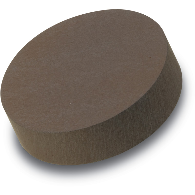
Bismuth Telluride ( Bi2Te3 ) Sputtering TargetBismuth Telluride (Bi₂Te₃) Sputtering Targets: Key Material Properties and Applications in Thin-Film ResearchBismuth Telluride (Bi₂Te₃) is a V-VI group semiconductor compound known for its exceptional thermoelectric properties at room temperature, ma...
Bismuth Telluride (Bi₂Te₃) Sputtering Targets: Key Material Properties and Applications in Thin-Film Research
Bismuth Telluride (Bi₂Te₃) is a V-VI group semiconductor compound known for its exceptional thermoelectric properties at room temperature,
making it one of the most widely studied materials for solid-state energy conversion and thin-film devices. With a melting point of approximately
575°C and a density of ~7.86 g/cm³, Bi₂Te₃ crystallizes in a rhombohedral structure (space group: R-3m). Its narrow bandgap of ~0.145 eV,
corresponding to the infrared spectrum around 4 μm, also supports applications in IR photodetection and optoelectronics.
Key Material Properties of Bi₂Te₃ Sputtering Targets
High Purity and Structural Control: Our Bi₂Te₃ sputtering targets are manufactured under strict controls, ensuring high purity
(with impurity analysis via GDMS or ICP spectroscopy) and fine grain structure. This is critical for reproducible film growth and
high-performance applications.
Controlled Crystallographic Orientation: When deposited under optimized conditions—such as specific substrate temperatures
and working pressures—Bi₂Te₃ films can achieve strong (00l) preferred orientation. This layered growth results in high in-plane
carrier mobility and exceptional electrical conductivity (exceeding 10⁵ S/m).
Excellent Thermoelectric Performance: Bi₂Te₃ thin films exhibit a high power factor (up to 42.5 μW/(cm·K²) for n-type systems)
and a notable Seebeck coefficient. Post-annealing in inert environments (e.g., 200 °C in N₂) further enhances electron mobility
and power factor, reaching values as high as 24.1 μW/K²cm.
Adaptable to Multiple Deposition Methods: Our targets are compatible with RF magnetron sputtering, co-sputtering,
and e-beam evaporation, allowing researchers to tailor stoichiometry, microstructure, and doping (e.g., with Ag or Se).
Applications of Bi₂Te₃ Thin Films in Advanced Research
Bi₂Te₃ films deposited via sputtering are enabling breakthroughs in several domains:
1. Flexible and Micro Thermoelectric Devices
Bi₂Te₃-based thin films are ideal for flexible thermoelectric generators (F-TEDs) and micro-Peltier coolers, especially in wearable
electronics and localized cooling of micro-optoelectronic components.
Thin-film thermocouples using p-Sb₂Te₃ / n-Bi₂Te₃ pairs have demonstrated temperature differences of ~15 K under low current input,
highlighting potential for on-chip thermal management.
2. Infrared Transparent Conductive Films
Bi₂Te₃ films combine notable mid-infrared transparency (up to 80% in the 1–5 μm range) with strong electrical conductivity
(resistivity as low as ~1.448×10⁻³ Ω·cm), making them promising as infrared transparent electrodes for IR photonics and detector integration.
3. High-ZT Thermoelectric Modules
By leveraging quantum confinement and interface effects in nanostructured films (e.g., layered or nanowire forms), researchers
have achieved ZT values up to 1.3 at 303 K in flexible printed films. This opens pathways to scalable, high-performance cooling and power generation.
4. Nanostructured and Composite Films
Templated or hybrid approaches, including the use of Te nanorods as "nano-binders," improve film densification, reduce thermal
conductivity (as low as 0.19 W/m·K), and enhance mechanical flexibility—all without compromising electrical properties.
Why Choose Our Bi₂Te₃ Sputtering Targets?
We provide precision-engineered Bi₂Te₃ sputtering targets with the following advantages:
Customization: Targets can be tailored in composition, doping, dimensions, and backing plates to match specific deposition systems (e.g., RF magnetron sputtering) and research needs.
High Material Quality: Each target is produced via a controlled process—melting, purification, forging, machining—
and includes comprehensive quality documentation.
If you are working on thermoelectric films, IR photonic devices, or flexible electronics, our Bi₂Te₃ targets offer a reliable and
high-performance material solution. For technical specifications, custom orders, or collaboration inquiries, please contact us.
For questions about target material or anything we can hlep, please click here.
| Specifications | |||
| Material Type | Bismuth Telluride | ||
| Symbol | Bi2Te3 | ||
| Purity | 99.99% | ||
| Size | 1.00" Dia. x 0.125" Thick ~8.00" Dia x 0.250" Thick / Custom | ||
| Package Unit | 1pc | ||
Warmly welcome new and regular customers' inquiry!
Contact Us
ICP:鲁ICP备18046268号-1 鲁公网安备37048102006786号 XMLMap
Address:New Business Building, Tengzhou City, China
