


Hotline
+86 13310681862

Description:
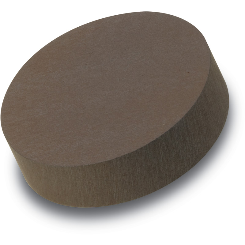
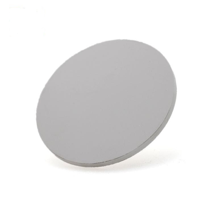
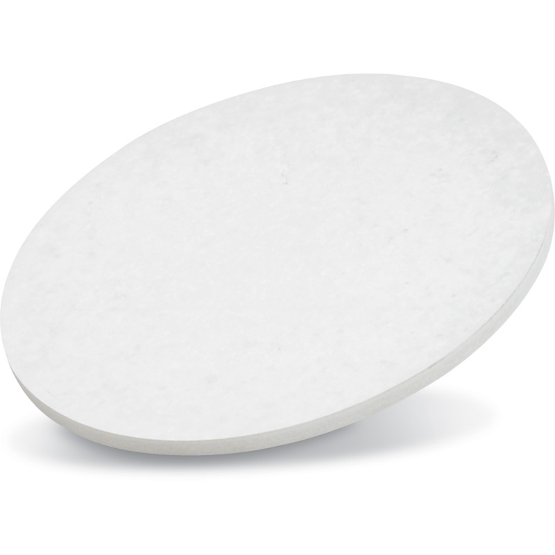
Bismuth oxide (Bi2O3) Sputtering TargetBismuth Oxide (Bi₂O₃) sputtering targets are a critical enabling material for thin-film deposition across a diverse range of high-tech industries. Valued for its unique combination of optical, electrical, and ionic properties, Bi₂O3 films are pushing the bou...
Bismuth Oxide (Bi₂O₃) sputtering targets are a critical enabling material for thin-film deposition across a diverse range
of high-tech industries. Valued for its unique combination of optical, electrical, and ionic properties, Bi₂O3 films are pushing
the boundaries of performance in energy, optics, and electronics.
Our high-purity, high-density Bismuth Oxide targets are engineered for superior performance in Magnetron Sputtering,
Pulsed Laser Deposition (PLD), and E-Beam Evaporation processes, ensuring consistent, high-quality film production.
Key Applications of Bi₂O₃ Thin Films:
1. Solid Oxide Fuel Cells (SOFCs) – High-Performance Electrolytes
Benefit: Delta-phase (δ) Bi₂O₃ possesses the highest known oxygen ion conductivity of any material,
enabling ultra-efficient ion transport.
Application: Thin-film electrolytes deposited from Bi₂O₃ targets significantly lower the operating temperature of SOFCs,
enhancing efficiency, startup time, and long-term system durability.
2. Advanced Optical Coatings
Benefit: Exceptionally high refractive index (~2.45 - 2.65 in the visible spectrum) and excellent transparency.
Application: Ideal for manufacturing sophisticated multi-layer optical filters, including:
Distributed Bragg Reflectors (DBRs)
Anti-Reflective (AR) Coatings
High-Reflectivity Mirrors
Planar Optical Waveguides
3. Next-Generation Memory & Electronic Devices
Benefit: Exhibits strong Resistive Switching (RS) behavior and high dielectric constant.
Application: Serves as a key active layer in Resistive Random-Access Memory (RRAM or ReRAM) for non-volatile data storage.
Also used in research as a high-κ dielectric layer and for developing ferroelectric thin films like BTO.
4. Visible-Light Photocatalysis
Benefit: Optimal narrow bandgap (~2.8 eV) for efficient absorption of visible light.
Application: Creates highly active photocatalytic films for:
Water Purification and degradation of organic pollutants.
Self-Cleaning and Antimicrobial Surfaces.
Photoelectrochemical (PEC) Water Splitting for hydrogen generation.
5. Gas and Chemical Sensing
Benefit: Electrical properties are highly sensitive to the surrounding gas atmosphere.
Application: Used in thin-film sensors for detecting various gases (e.g., H₂, CO, NOx) and as a sensing layer for pH electrodes.
For questions about target material or anything we can hlep, please click here.
| Specifications | |||
| Material Type | Bismuth Oxide | ||
| Symbol | Bi2O3 | ||
| Purity | 99.99% | ||
| Size | 1.00" Dia. x 0.125" Thick ~8.00" Dia x 0.250" Thick / Custom | ||
| Package Unit | 1pc | ||
Warmly welcome new and regular customers' inquiry!
Contact Us
ICP:鲁ICP备18046268号-1 鲁公网安备37048102006786号 XMLMap
Address:New Business Building, Tengzhou City, China
