


Hotline
+86 13310681862

Description:
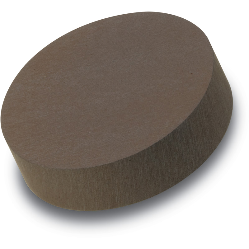
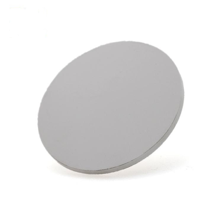
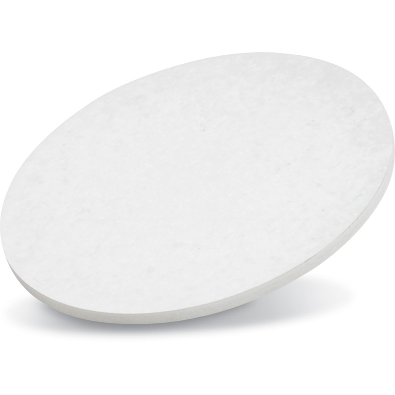
Molybdenum Trioxide (MoO₃) Sputtering TargetMolybdenum trioxide (MoO₃) sputtering targets are engineered to meet the rigorous demands of academic and industrial thin-film research. With ultra-high purity (>99.99%), exceptional stoichiometric control, and uniform density, these targets are ideal...
Molybdenum trioxide (MoO₃) sputtering targets are engineered to meet the rigorous demands of academic and industrial thin-film research.
With ultra-high purity (>99.99%), exceptional stoichiometric control, and uniform density, these targets are ideal for PVD
(magnetron sputtering, thermal evaporation) and ALD (atomic layer deposition) processes.
Key applications in research laboratories include:
Thin-Film Transistors (TFTs): Optimizing charge transport layers for flexible displays, wearable sensors, and IoT-compatible electronics.
Transparent Electrodes: Depositing MoO₃-based interfacial layers to enhance efficiency in organic LEDs (OLEDs)
and perovskite light-emitting diodes (PeLEDs).
2D Material Integration: Modifying interfaces in graphene, MoS₂, or WS₂ heterostructures for tailored electronic properties.
Perovskite Solar Cells: Serving as efficient hole-selective contacts to minimize recombination losses and improve device stability.
Photoelectrochemical (PEC) Systems: Fabricating catalytic coatings for hydrogen evolution or CO₂ reduction studies.
Solid-State Batteries: Investigating MoO₃ thin films as anode/cathode interlayers to enhance ion transport kinetics.
Smart Windows: Developing electrochromic/thermochromic films for dynamic optical modulation in energy-efficient buildings.
Corrosion-Resistant Barriers: Studying ultrathin MoO₃ coatings for aerospace alloys or biomedical implants under extreme conditions.
Memristors: Exploring MoO₃-based resistive switching layers for neuromorphic computing architectures.
Nanoscale Sensors: Designing gas-sensitive or plasmonic films for ultrasensitive detection of environmental pollutants.
Bandgap Engineering: Tuning MoO₃’s electronic structure (n-type semiconductor, ~3.0 eV bandgap) via doping or heterojunction design.
In-Situ Growth Studies: Leveraging ALD compatibility for atomic-level control in epitaxial thin-film synthesis.
For questions about target material or anything we can hlep, please click here.
| Specifications | |||
| Material Type | Molybdenum Oxide | ||
| Symbol | MoO3 | ||
| Purity | 99.99% | ||
| Size | 1.00" Dia. x 0.125" Thick ~8.00" Dia x 0.250" Thick / Custom | ||
| Package Unit | 1pc | ||
| Theoretical Density (g/cc) | 4.69 | ||
| Melting Point (°C) | 795 °C | Sputter | RF, RF-R |
| Type of Bond | Indium, Elastomer | Max Power Density (Watts/Square Inch) | -- |
| Comments | Slight oxygen loss. | Color/Appearance | White to Pale Yellow, Crystalline Solid. |
Warmly welcome new and regular customers' inquiry!
Contact Us
ICP:鲁ICP备18046268号-1 鲁公网安备37048102006786号 XMLMap
Address:New Business Building, Tengzhou City, China
