


Hotline
+86 13310681862

Description:
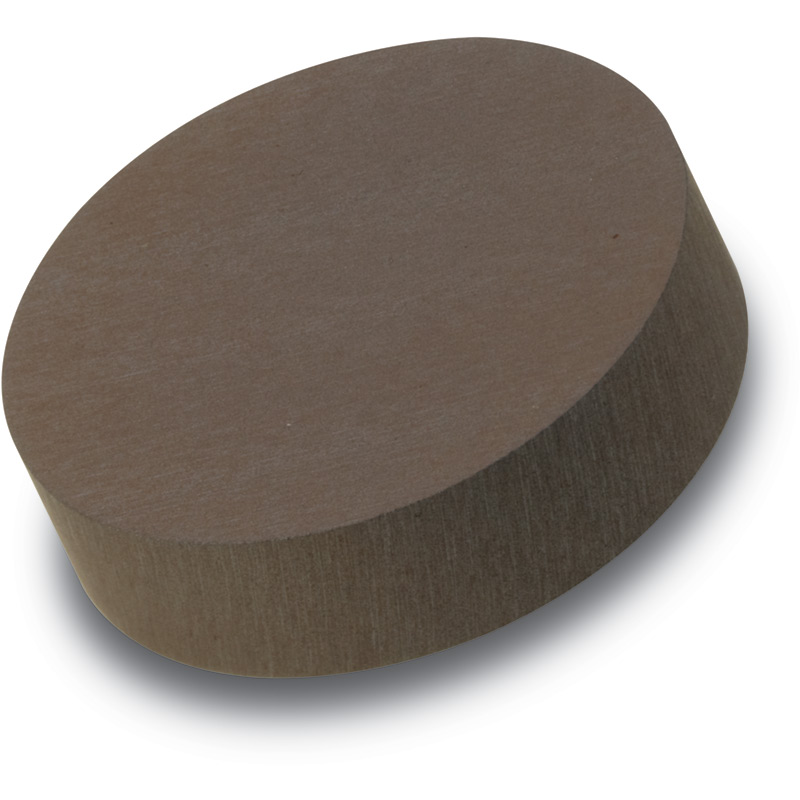
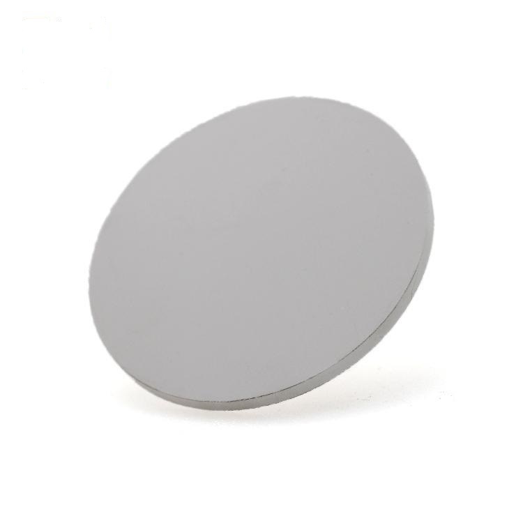
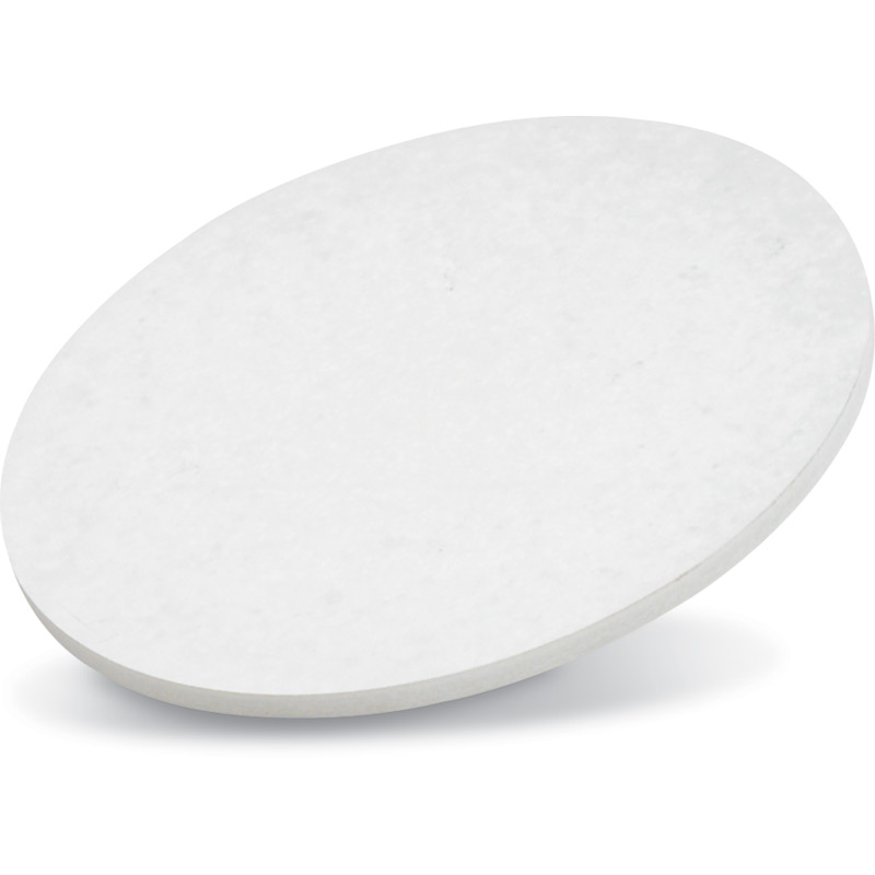
Tin Sulfide (SnS2) Sputtering TargetTin Sulfide Sputtering Targetsare used for multilayer thin film....
Bulk orthorhombic SnS has a density of 5.22 g cm−3 and a melting point of 882 °C. Bulk band gap energies ranging from 1.20 to 1.37 eV have been reported, with some outlying values as low as 1.07 eV. SnS possesses a thermal conductivity around 1 W m−1 K−1 and a Seebeck coefficient in the range 300–500 µV K−1.

| Specifications | |||
| Material Type | Tin Sulfide | ||
| Symbol | SnS | ||
| Purity | 99.99% | ||
| Size | 1.00" Dia. x 0.125" Thick ~8.00" Dia x 0.250" Thick / Custom | ||
Tin(II) sulfide has emerged as an alternative solar absorber material to conventional thin film absorbers such as cadmium telluride (CdTe) and copper indium gallium selenide (CIGS), due to several properties including biological non-toxicity.
Tin and sulfur are also both environmentally benign elements which are cheap and abundant in nature. SnS has an ideal bandgap for solar absorption (1.3 eV for bulk), a high absorbance coefficient >10−4 cm−1, Hall mobility up to 100 cm2 Vs−1 or higher, and tuneable carrier densities in the range of 1015 to 1018 cm−3.
Due to these exciting properties, it has been incorporated into thin film solar cell architecture alongside a range of electron and hole transporting materials.
Additionally, SnS has also been used as a substitute for platinum as a counter electrode (CE) in dye-sensitised solar cells (DSSCs).
The use of SnS is becoming more widespread and includes applications in photodetectors, Li-ion and Na-ion batteries, and sensors, amongst others.
For questions about target material or anything we can hlep, please click here.
Warmly welcome new and regular customers' inquiry!
Contact Us
ICP:鲁ICP备18046268号-1 鲁公网安备37048102006786号 XMLMap
Address:New Business Building, Tengzhou City, China
