


Hotline
+86 13310681862

Description:
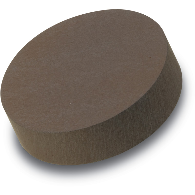
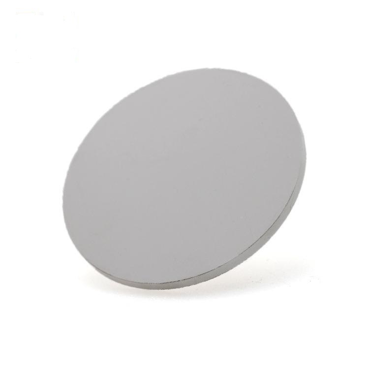
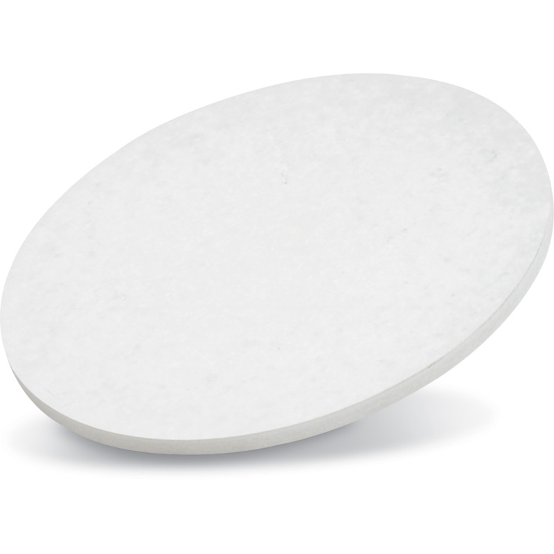
Chromium Silicide (CrSi2 ) Sputtering Targets used for thin film deposition...
Such properties of CrSi2 as the high temperature of melting, the resistance to oxidation and the capability of standing a considerable
deformation make it a prospective material
under the conditions of the energy influences. Earlier, CrSi2 layers were mainly applied as the barriers of Schottky diodes.
At present, the CrSi2 layers are also used as a joint between silicon and the working element in the integrated circuits and the sensors
owing to the low transient resistance and the semiconductor properties.
This peculiarity in combination with a good compatibility with the regular silicon technologies makes it possible to successfully apply
CrSi2 in the thermoelectric and photoelectric devices. The narrow prohibited zone makes it suitable for application in the converters
and sensors in micro- and nanoelectronics.
For questions about target material or anything we can hlep, please click here.
| Specifications | |||
| Material Type | Chromium Silicide | ||
| Symbol | CrSi2 | ||
| Purity | 99.95% | ||
| Size | 1.00" Dia. x 0.125" Thick ~8.00" Dia x 0.250" Thick / Custom | ||
| Package Unit | 1pc | ||
| Theoretical Density (g/cc) | 5.5 | ||
| Color/Appearance | Silvery, Metallic | Sputter | RF |
| Melting Point (°C) | 1,490 | Type of Bond | Indium, Elastomer |
Warmly welcome new and regular customers' inquiry!
Contact Us
ICP:鲁ICP备18046268号-1 鲁公网安备37048102006786号 XMLMap
Address:New Business Building, Tengzhou City, China
