


Hotline
+86 13310681862

Description:
In2S3 is considered a promising semiconductor material for many applications including; optoelectronic, photovoltaic, and photoelectrochemical solar cells....
In2S3 is layered with hexagonal, tetragonal, and spinal structures. One of the most unique feature properties of In2S3 is the bandgap energy. In2S3 is a nontoxic material of n-type semiconductor with an energy band gap of 2.0–2.8 eV, depending upon the preparation technique, and having a high transmittance in the visible part of the spectrum.
In2S3 is considered a promising semiconductor material for many applications including; optoelectronic, photovoltaic, and photoelectrochemical solar cells.
The reasons behind the potential applications of In2S3 are its stability, transparency, wider bandgap energy, and photo conducting behavior. In2S3 exhibits different phase structures like α, β, and γ depending on the preparing conditions. The most stable phase among them at room temperature is the β-In2S3 phase which was found to be a stable crystalline phase with a tetragonal structure.
In2S3 has emerged as a promising low-hazard buffer (or window) material, and has proven to improve the properties of the solar cells, while reducing toxicity.

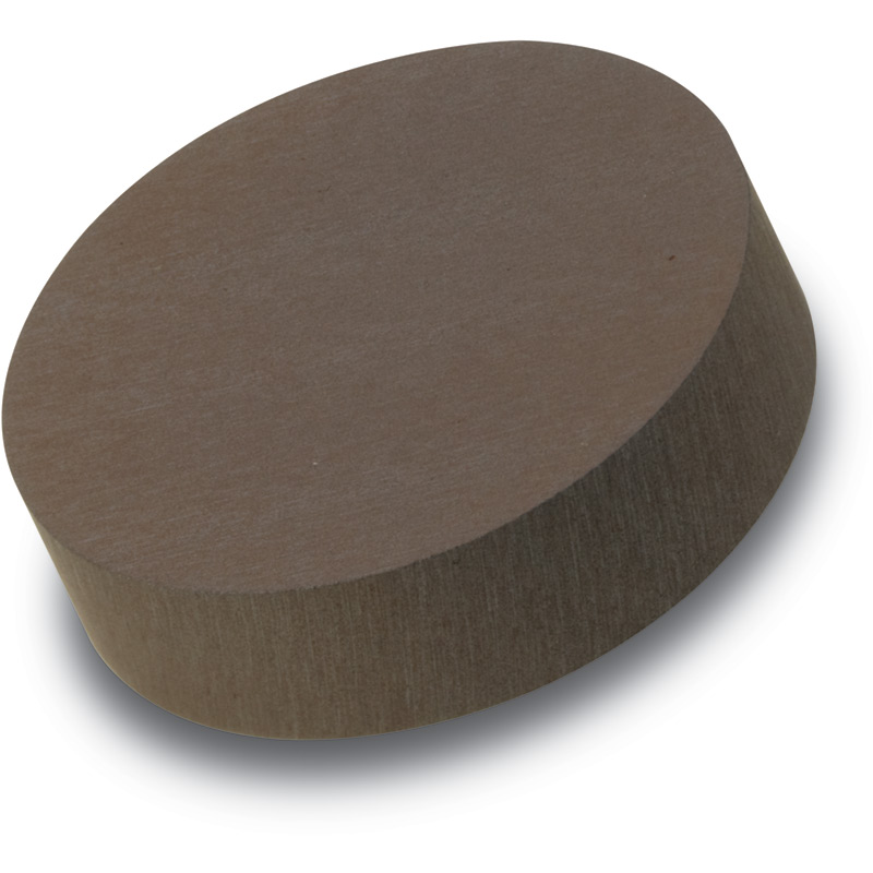
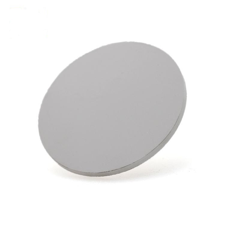
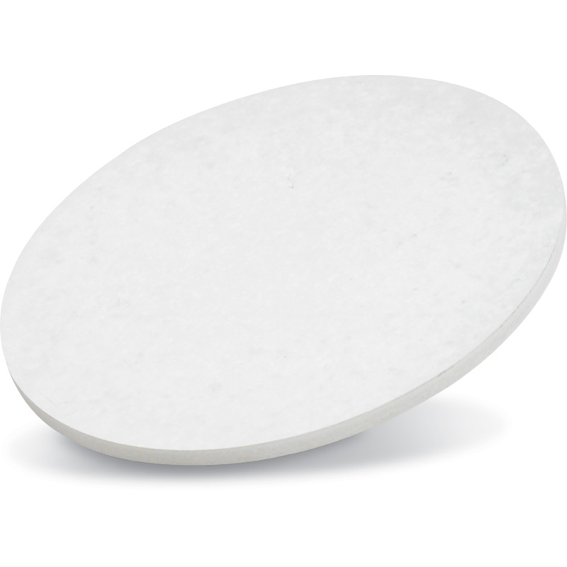
| In2S3 sputtering Target | |
| Formula | In2S3 |
| Density (g/mL,25℃) | 4.45 |
| Melting Point (℃) | 1050 |
| Purity | 99.99% |
| Sputter | RF |
Warmly welcome new and regular customers' inquiry!
Contact Us
ICP:鲁ICP备18046268号-1 鲁公网安备37048102006786号 XMLMap
Address:New Business Building, Tengzhou City, China
