


Hotline
+86 13310681862

Description:
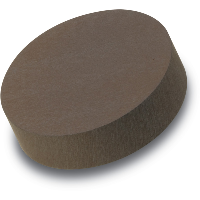
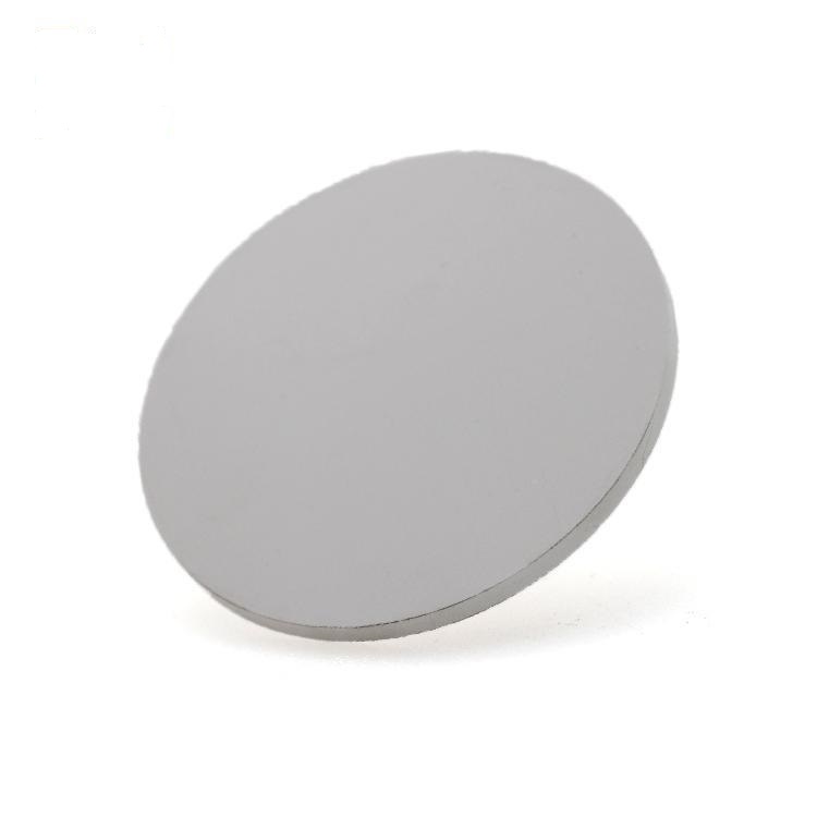
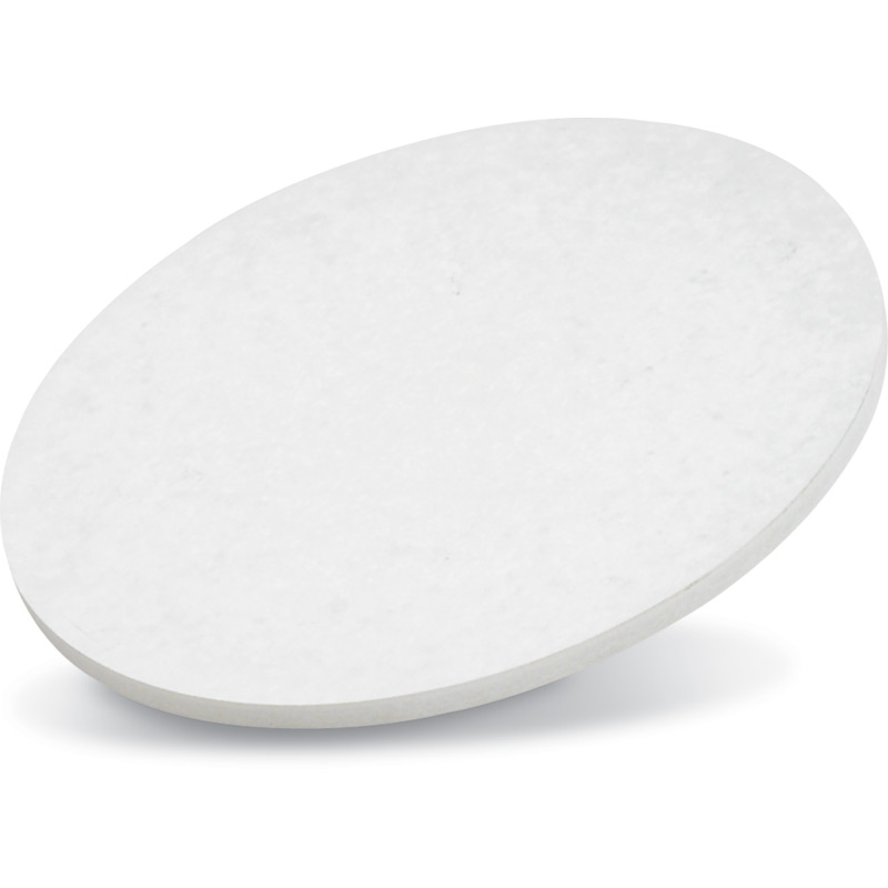
Cadmium Selenide CdSe Sputtering TargetsHigh-purity cadmium selenide (CdSe) sputtering targets (≥99.99% purity) are critical for advanced thin-film deposition in PVD (magnetron sputtering) and thermal evaporation systems. As a direct bandgap semiconductor (~1.74 eV), CdSe offers exceptional o...
High-purity cadmium selenide (CdSe) sputtering targets (99.99% purity) are critical for advanced thin-film deposition in PVD (magnetron sputtering)
and thermal evaporation systems. As a direct bandgap semiconductor (~1.74 eV), CdSe offers exceptional optoelectronic tunability,
making it indispensable for next-generation research in academia and industry. Below are its key applications:
1. Optoelectronics & Photovoltaics
Quantum Dot Synthesis: CdSe thin films serve as precursors for high-efficiency CdSe/CdS core-shell quantum dots, widely used in displays, LEDs,
and biological imaging.
Solar Cells: Integration into CIGS (CuInGaSe₂) thin-film solar cells as buffer layers or absorbers to enhance light-harvesting efficiency.
Photodetectors: Fabrication of visible-to-near-infrared (Vis-NIR) photodetectors for optical communication and sensing systems.
2. Nanoelectronics & Quantum Technologies
2D Heterostructures: Deposition of CdSe layers for hybrid structures with graphene, MoS₂, or perovskites to study charge transfer mechanisms.
Single-Photon Emitters: Development of nanoscale CdSe-based emitters for quantum cryptography and quantum computing research.
3. Infrared Optics & Coatings
IR Transparent Films: CdSe’s broad infrared transmission range (up to ~25 µm) enables coatings for thermal imaging lenses and IR sensor windows.
Anti-Reflective Coatings: Multi-layer designs for laser optics and aerospace-grade infrared systems.
4. Energy Conversion & Catalysis
Photoelectrochemical Water Splitting: CdSe films act as photocathodes for hydrogen generation studies due to their favorable band alignment.
CO₂ Reduction Catalysts: Thin-film electrodes for converting CO₂ into hydrocarbons under visible-light irradiation.
5. Biomedical & Sensor Applications
Bioimaging Probes: CdSe nanoparticles synthesized via thin-film precursors for fluorescent labeling in cellular imaging.
Gas Sensors: CdSe-based resistive sensors for detecting volatile organic compounds (VOCs) or environmental toxins.
For questions about target material or anything we can hlep, please click here.
| Specifications | |||
| Material Type | Cadmium Selenide | ||
| Symbol | CdSe | ||
| Purity | 99.99% | ||
| Size | 1.00" Dia. x 0.125" Thick ~8.00" Dia x 0.250" Thick / Custom | ||
| Package Unit | 1pc | ||
| Theoretical Density (g/cc) | 5.81 | ||
| Melting Point (°C) | >1,350 | Sputter | RF |
| Type of Bond | Indium, Elastomer | Max Power Density (Watts/Square Inch) | 20* |
Warmly welcome new and regular customers' inquiry!
Contact Us
ICP:鲁ICP备18046268号-1 鲁公网安备37048102006786号 XMLMap
Address:New Business Building, Tengzhou City, China
