


Hotline
+86 13310681862
Description:
Molybdenum Mo Sputtering TargetApplications of High-Purity Molybdenum (Mo) TargetsSemiconductor FabricationHigh-purity Mo targets are critical for sputter deposition of conductive barrier layers and interconnects in advanced semiconductor devices, ensuring low resistivity and robust electromigration...
High-purity Mo targets are critical for sputter deposition of conductive barrier layers and interconnects in advanced semiconductor devices,
ensuring low resistivity and robust electromigration resistance in nanoscale integrated circuits (ICs).
Used in thin-film transistor liquid crystal displays (TFT-LCDs) and OLEDs to deposit gate electrodes and pixel electrodes, Mo enhances electrical
conductivity and stability in high-resolution screens.
Essential for copper indium gallium selenide (CIGS) and cadmium telluride (CdTe) thin-film solar cells, Mo serves as a highly adherent back
contact layer, optimizing carrier collection and long-term durability.
Deposited via physical vapor deposition (PVD), Mo coatings provide extreme UV (EUV) reflectivity for lithography systems and
wear-resistant surfaces for aerospace components exposed to high-temperature, corrosive environments.
Mo targets are utilized in X-ray tube anodes for mammography and diagnostic imaging, leveraging their high melting point (2,623°C)
and efficient X-ray emission at lower kVp settings.
Sputtered Mo films enable low-emissivity (Low-E) coatings on energy-efficient windows, reducing infrared radiation while maintaining
visible light transparency.
Mo targets support electron beam melting (EBM) and laser powder bed fusion (LPBF) processes to produce high-strength,
heat-resistant components for aerospace and defense.
Used in sputtered buffer layers for high-temperature superconducting (HTS) tapes (e.g., YBCO), Mo ensures lattice matching and
thermal stability in power grid and MRI magnet applications.
Mo thin films are engineered for microelectromechanical systems (MEMS) and gas sensors, offering exceptional thermal and
chemical stability in harsh operating conditions.
Ultra-high purity (≥99.95%) minimizes contamination in precision thin-film processes.
Superior thermal/electrical conductivity and mechanical strength under extreme environments.
Customizable geometries (rotary, planar) and surface finishes for optimized deposition uniformity.
For questions about target material or anything we can hlep, please click here.
| Specifications | |||
| Material Type | Molybdenum | ||
| Symbol | Mo | ||
| Purity | 99.95% | ||
| Size | 1.00" Dia. x 0.125" Thick ~8.00" Dia x 0.250" Thick / Custom | ||
| Package Unit | 1pc | ||
| Theoretical Density (g/cc) | 10.2 | Z Ratio | 0.257 |
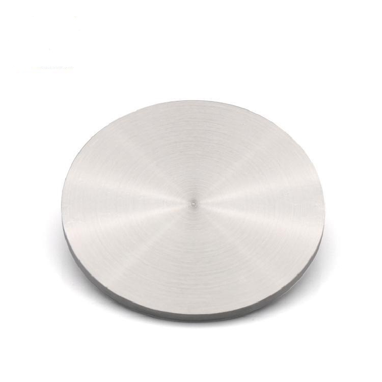
| Color/Appearance | Grey, Metallic | Sputter | DC |
| Atomic Weight | 95.96 | Max Power Density (Watts/Square Inch) | 150* |
| Melting Point (°C) | 2,617 | Type of Bond | Indium, Elastomer |
| Coefficient of Thermal Expansion | 4.8 x 10⁻⁶/K | Comments | Films smooth, hard. Careful degas required. |
| Thermal Conductivity | 139 W/m.k | ||
Warmly welcome new and regular customers' inquiry!
Contact Us
ICP:鲁ICP备18046268号-1 鲁公网安备37048102006786号 XMLMap
Address:New Business Building, Tengzhou City, China
