


Hotline
+86 13310681862

Description:
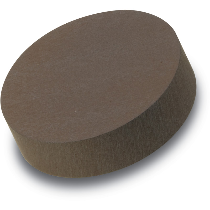
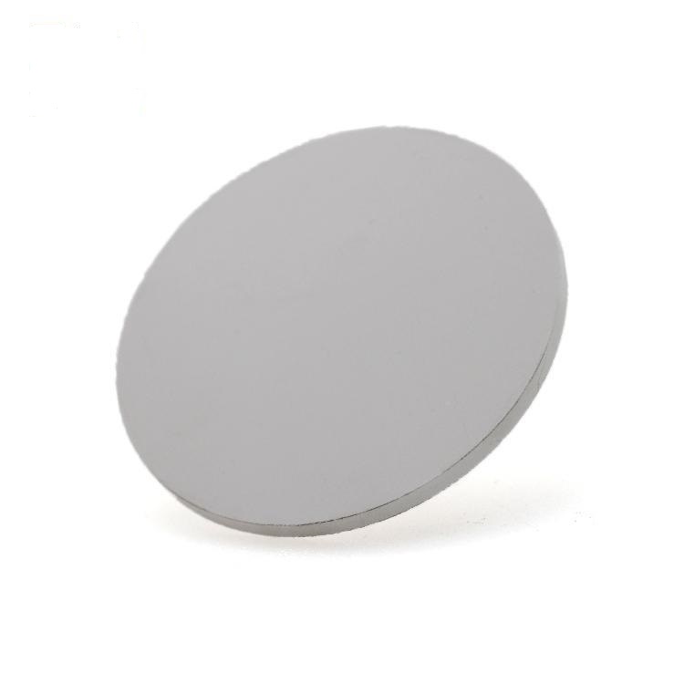
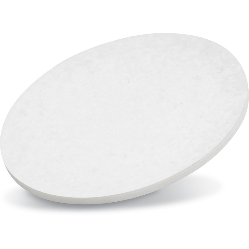
Silicon Carbide Sputtering TargetsSilicon Carbide Target Application Areas1. Semiconductor and Electronic DevicesPower devices: SiC thin films are used in the manufacture of high-voltage, high-temperature semiconductor devices (e.g., MOSFETs, Schottky diodes) to improve energy conversion efficiency....
Power devices: SiC thin films are used in the manufacture of high-voltage, high-temperature semiconductor devices
(e.g., MOSFETs, Schottky diodes) to improve energy conversion efficiency.
RF devices: In high-frequency communications (5G, radar), SiC's high electron saturation speed supports higher frequency operation.
UV Optoelectronic Devices: Used in UV detectors, LED substrates, especially outstanding in the short wavelength UV field.
Optical coatings: high refractive index and corrosion resistance make it suitable for infrared windows, laser lens protection layer.
Machine Tool Coatings: Extend the life of cutting tools, molds and dies (hardness up to 25-30 GPa).
Aerospace components: anti-erosion and anti-oxidation coatings for turbine blades, engine components.
Nuclear reactor materials: as a protective layer against radiation and high temperatures.
High-temperature sensors: thin films for pressure or gas sensing at extreme temperatures.
Fuel cell: as a proton exchange membrane or bipolar plate coating to enhance corrosion resistance.
Lithium-ion battery: electrode protection layer, inhibit dendrite growth, improve safety.
For questions about target material or anything we can hlep, please click here.
| Specifications | |||
| Material Type | Silicon Carbide | ||
| Symbol | SiC | ||
| Purity | 99.9% | ||
| Size | 1.00" Dia. x 0.125" Thick ~8.00" Dia x 0.250" Thick / Custom | ||
| Package Unit | 1pc | ||
| Theoretical Density (g/cc) | 3.22 | ||
| Melting Point (°C) | 2700 | Sputter | RF |
| Type of Bond | Indium, Elastomer | Max Power Density (Watts/Square Inch) | 20* |
Warmly welcome new and regular customers' inquiry!
Contact Us
ICP:鲁ICP备18046268号-1 鲁公网安备37048102006786号 XMLMap
Address:New Business Building, Tengzhou City, China
