


Hotline
+86 13310681862
Description:
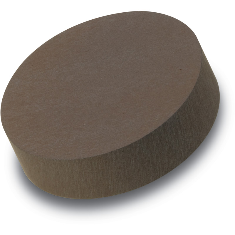
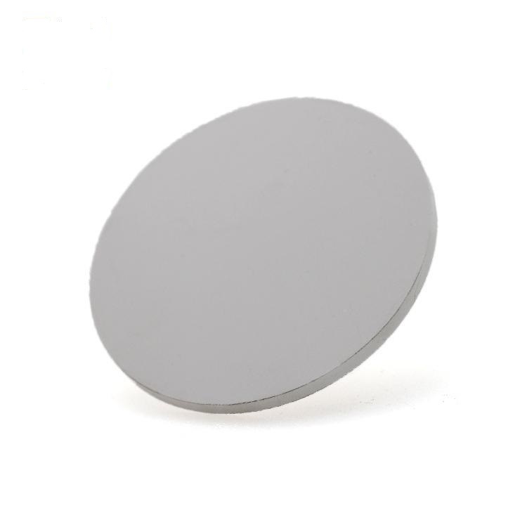
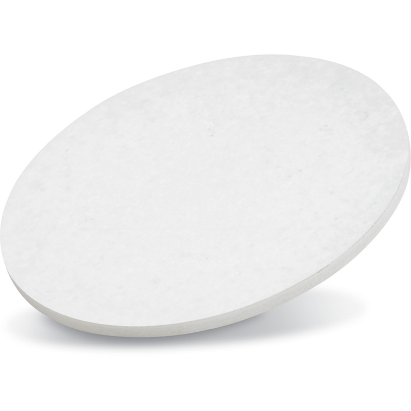
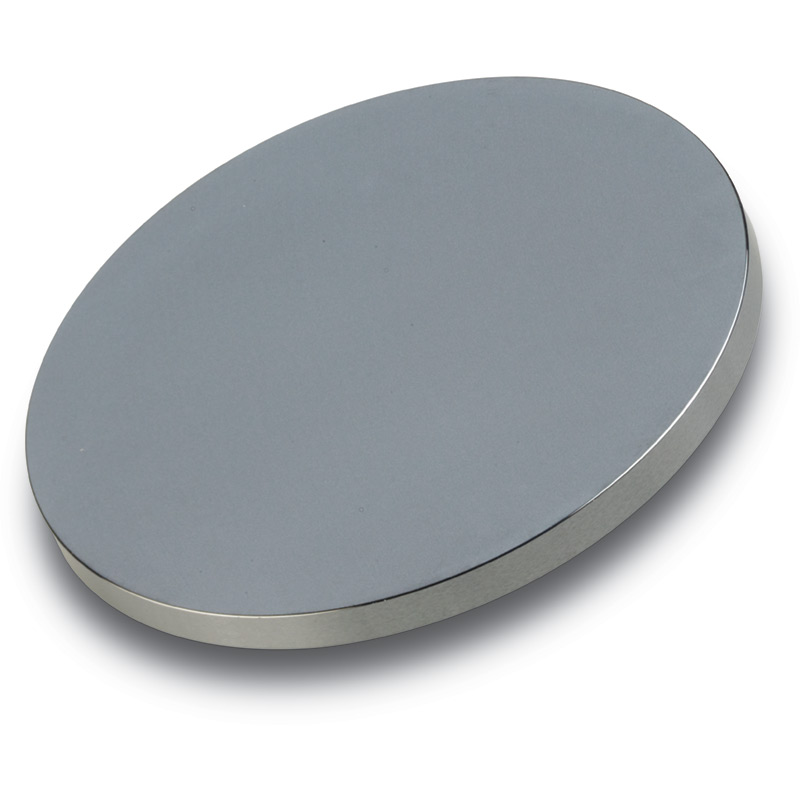
The N-type Silicon sputtering target is used for thin film deposition, decoration, semiconductor, display, LED and photovoltaic devices, functional coating as nicely as other optical information storage space industry, glass coating industry like car glass and architectural glass, optical communicat...
The N-type Silicon sputtering target is used for thin film deposition, decoration, semiconductor, display, LED and photovoltaic devices, functional coating as nicely as other optical information storage space industry, glass coating industry like car glass and architectural glass, optical communication, etc.
Other applications of silicon are:Solar cells, Transistors, Semiconductors, Rectifiers and other solid-state devices that are used widely in the electronics and space sectors.
For questions about target material or anything we can hlep, please click here.
| Specifications | |||
| Material Type | Silicon | ||
| Symbol | Si | ||
| Purity | (P type/ N type/ Intrinsic Type ) 99.999% | ||
| Size | 1.00" Dia. x 0.125" Thick ~8.00" Dia x 0.250" Thick / Custom | ||
| Package Unit | 1pc | ||
| Atomic Weight | 28.0855 | Z Ratio | 0.712 |
| Color/Appearance | Dark Gray with a Bluish Tinge, Semi-Metallic | Sputter | RF |
| Thermal Conductivity | 150 W/m.K | Max Power Density(Watts/Square Inch) | 20* |
| Melting Point (°C) | 1,410 | Type of Bond | Indium, Elastomer |
| Coefficient of Thermal Expansion | 2.6 x 10⁻⁶/K | Max Power Density(Watts/Square Inch) | 100* |
| Theoretical Density (g/cc) | 2.32 | Comments | Alloys with W; use heavy W boat. SiO produced. |
Warmly welcome new and regular customers' inquiry!
Contact Us
ICP:鲁ICP备18046268号-1 鲁公网安备37048102006786号 XMLMap
Address:New Business Building, Tengzhou City, China
