


Hotline
+86 13310681862
Description:
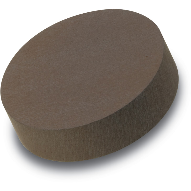
CdS Sputtering Targetsare used for thin film deposition....
Cadmium sulfide (CdS) is a semiconducting material utilized in a variety of applications. The wide band gap, low
absorption loss, compact crystallographic cell structure and electronic affinity makes CdS is a promising optoelectronic
device for making solar cell CISe and InP. Thin films of CdS have received widespread attention in the direction of other
device applications such as including electrochemical cells, gas sensors, and metal-Schottky barrier cells. It is mainly
used as an optical window material. Nanoparticles of CdS doped with other semiconductor materials working as photo
sensor detection, Light emitting diodes (LED), Semiconductor lasers, Thin films transistors, Photo detectors,
Photoluminescence, Photosensitization and Photocatalytic properties solar cell and gas sensor. CdS is an important
room temperature band gap of ∼2.42 eV (512 nm) and the potential applications of CdS have been used as a window
layer in solar cell together with narrow band gap materials.
For questions about target material or anything we can hlep, please click here.
| Specifications | |||
| Material Type | Cadmium Sulfide | ||
| Symbol | CdS | ||
| Purity | 99.99% | ||
| Size | 1.00" Dia. x 0.125" Thick ~8.00" Dia x 0.250" Thick / Custom | ||
| Package Unit | 1pc | ||
| Theoretical Density (g/cc) | 4.82 | ||
| Melting Point (°C) | 1,750 | Sputter | RF |
| Type of Bond | Indium, Elastomer | Max Power Density (Watts/Square Inch) | 20* |
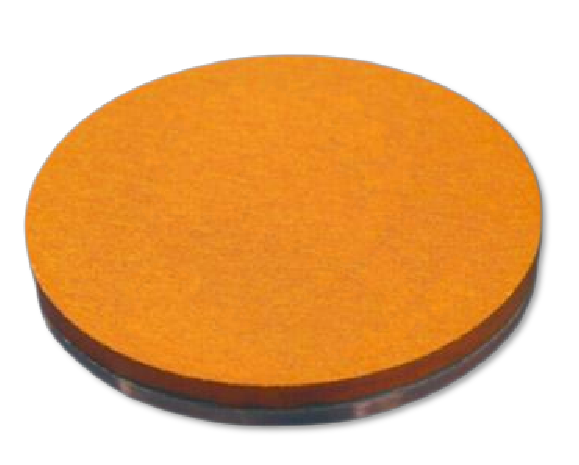
| Comments | Sticking coefficient affected by substrate. | Color/Appearance | Yellow to Orange, Crystalline Solid |
Warmly welcome new and regular customers' inquiry!
Contact Us
ICP:鲁ICP备18046268号-1 鲁公网安备37048102006786号 XMLMap
Address:New Business Building, Tengzhou City, China
