


Hotline
+86 13310681862

Description:
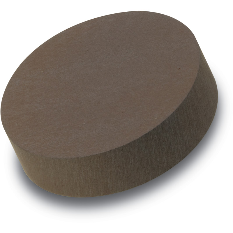
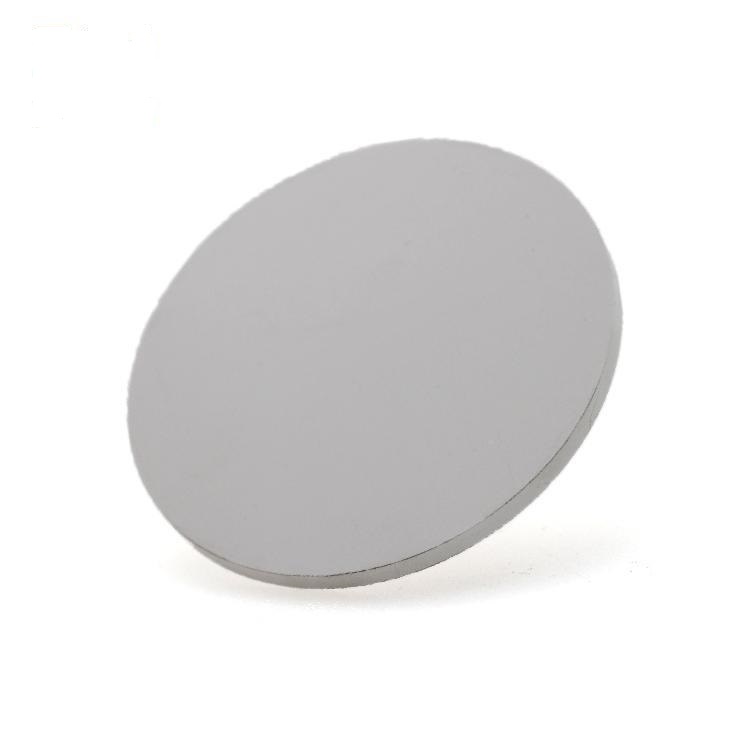
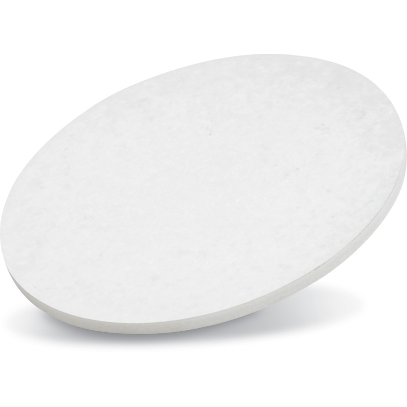
High-Purity Selenium (Se) Sputtering TargetsHigh-purity selenium (Se) sputtering targets exhibit unique semiconductor and photoelectric properties, making them essential for advanced thin-film research. Key characteristics include:Ultra-High Purity: ≥99.999% (5N) purity ensures minimal impurity int...
High-purity selenium (Se) sputtering targets exhibit unique semiconductor and photoelectric properties, making them essential for advanced thin-film research.
Key characteristics include:
Ultra-High Purity: ≥99.999% (5N) purity ensures minimal impurity interference, critical for high-performance optoelectronic and semiconductor applications.
Crystalline Structure: Trigonal crystal structure (space group P3<sub>1</sub>21) with anisotropic electrical and optical behavior, enabling tailored thin-film properties.
Physical Properties:
Density: 4.81 g/cm³ at 20°C.
Melting point: 221°C; Sublimation point: 685°C.
Bandgap: ~1.74 eV (amorphous) to ~1.89 eV (crystalline), suitable for infrared and visible light applications.
Electrical Properties: High photoconductivity and carrier mobility (up to 0.7 cm²/V·s), ideal for photodetectors and photovoltaic devices.
Sputtering Process Parameters
To achieve high-quality selenium thin films, precise control of sputtering conditions is critical:
Power and Pressure:
DC/RF magnetron sputtering is recommended, with power density maintained at 2–5 W/cm² to prevent thermal decomposition of Se.
Argon gas pressure: 0.5–1.0 Pa, balancing deposition rate (5–15 nm/min) and film uniformity.
Substrate Temperature: Optimized at 80–150°C to enhance crystallinity while avoiding Se sublimation.
Target Bonding: Oxygen-free copper (OFC) or molybdenum backing plates (2–4 mm thickness) ensure efficient heat dissipation and mechanical stability.
Pre-sputtering Treatment: Surface polishing (Ra <0.2 μm) and argon plasma cleaning to eliminate oxide layers and particulate contamination.
Post-Deposition Annealing: Optional thermal treatment (150–200°C in N₂ atmosphere) to improve film stoichiometry and reduce defects.
Application Directions
Selenium targets are pivotal in cutting-edge research and industrial applications:
Optoelectronics:
Fabrication of photodetectors and infrared sensors, leveraging Se’s narrow bandgap and high photoresponsivity.
Integration with Bi<sub>2</sub>Se<sub>3</sub> topological insulators for high-speed quantum devices and spintronic applications.
Energy Technologies:
Thin-film solar cells (e.g., Cu<sub>2</sub>ZnSn(S,Se)<sub>4</sub>), where Se doping optimizes band alignment and reduces interfacial recombination.
Thermoelectric materials (e.g., Bi<sub>2</sub>Te<sub>3</sub>-Se alloys), enhancing ZT values via carrier concentration modulation.
Advanced Coatings:
Anti-reflective and protective layers for infrared optics, utilizing Se’s transparency in the 1–20 μm wavelength range.
Semiconductor Research:
Deposition of chalcogenide phase-change materials (e.g., Ge-Sb-Se) for non-volatile memory and neuromorphic computing.
Why Choose Our Se Targets?
Our selenium targets are synthesized via zone refining and vacuum distillation, achieving sub-ppm metallic impurities (e.g., Fe, Cu <1 ppm).
Custom geometries (discs, rectangular plates) and ISO 9001-certified quality control ensure reproducibility for academic and industrial R&D.
For questions about target material or anything we can hlep, please click here.
| Specifications | |||
| Material Type | Selenium | ||
| Symbol | Se | ||
| Purity | 99.99% | ||
| Size | 1.00" Dia. x 0.125" Thick ~8.00" Dia x 0.250" Thick / Custom | ||
| Package Unit | 1pc | ||
| Theoretical Density (g/cc) | 4.81 | Sputter | DC |
| Melting Point (°C) | 217 | ||
Warmly welcome new and regular customers' inquiry!
Contact Us
ICP:鲁ICP备18046268号-1 鲁公网安备37048102006786号 XMLMap
Address:New Business Building, Tengzhou City, China
